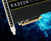
 AMD’s Vega graphics processors, featuring what the company has called Next-Generation Compute Units, have some major architectural changes – but will that translate into improved real-world performance? AMD has officially taken the wraps off its next-generation Vega graphics processor architecture, pointing to the improvements it hopes will help it win back market share lost to discrete graphics leader Nvidia.
Vega, due to launch early this year and appearing first in the company’s Radeon Instinct accelerator family , is being positioned by the company as being a major leap over previous generation graphics processors. In support of this claim, the company has treated the tech press to a technological overview of just why Vega should have a place in everything from gaming rigs to high-performance computing projects.
The company’s promises for Vega begin boldly, with the claim that it includes ‘ the world’s most scalable GPU memory architecture ‘. Using High Bandwidth Memory 2 (HBM2), the company is claiming a doubled bandwidth per pin and eight-fold capacity increase per stack, along with a halved footprint compared with off-chip GDDR5 memory.


