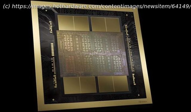
NVIDIA CEO Jensen Huang opened GTC 2024 by announcing Blackwell, the most powerful AI chip ever made.
Some people have claimed that AI is a fad, or a flash in the pan. It’s easy to understand the perspective; the hype around the explosion of generative AI feels similar to the hype around previous fads, like 3D TVs or the metaverse. AI isn’t a fad, though. It is already transforming every single part of the tech industry, and it’s about to start renovating the rest of the world, too. Right at the forefront of the AI revolution is NVIDIA, of course.
At GTC tonight, NVIDIA CEO Jensen Huang got on stage in his trademark leather jacket to make a multitide of announcements. Arguably the most important of them were the reveal of the Blackwell GPU architecture as well as NVIDIA’s first-party systems that it will power. The image at the top is of the Blackwell-based B200 Tensor GPU, while the „GB200“ moniker applies primarily to the GB200 Superchip, pictured here:NVIDIA’s Blackwell GPU Architecture Revealed
The GB200 includes a pair of Blackwell GPUs mated both to each other and to a 72-core „Grace“ CPU. The Blackwell GPUs have their own HBM3e memory, up to 192 GB apiece, while the Grace CPU can have up to 480GB of LPDDR5X memory attached. The whole thing is connected with the new 5th-generation NVLink, but we’ll talk more about that in a bit. First, let’s look a little deeper at the Blackwell GPU itself.
NVIDIA has complained for a few generations about being limited to the size of the reticle of TSMC’s lithography machines. How did they work around this? As it turns out, the answer is to link two chips together with a new interface. The full-power Blackwell GPU is indeed two „reticle-sized dies“ attached with the proprietary „NV-HBI“ high-bandwidth interface. NVIDIA says that the connection between the two pieces of silicon operates at up to 10 TB/second and offers „full performance with no compromises.“
The house that GeForce built makes many bold claims about Blackwell’s capabilities, including that it can train new AIs at four times the speed of Hopper, that it can perform AI inference at thirty times the speed of the previous-generation parts, and that it can do this while improving energy efficiency by 2500%. That’s a 25x improvement, if you do the math.
Of course, if you’re doing something 30 times faster and your energy efficiency went up by 25 times, then you’re actually using more power, and that’s indeed the case here. Blackwell can draw up to 1,200 watts per chip, which is what happens when you increase the transistor count by 2.5x over the previous generation without a die shrink. Blackwell is built on what NVIDIA calls „4NP“, a customized TSMC process tailored specifically for NVIDIA’s parts. While it’s likely to be improved over the „4N“ process used for Hopper, it doesn’t seem to be a compelte overhaul, so what NVIDIA has achieved is impressive to be sure.
NVIDIA says that there are six primary breakthroughs that have enabled Blackwell to become „a new class of AI superchip.“ These breakthroughs are the extraordinarily high transistor count, the second-generation transformer engine, the 5th-generation NVLink, the new Reliability, Availability, and Serviceability (RAS) Engine, additional capabilities for „Confidential Computing“ including TEE-I/O capability, and a dedicated decompression engine capable of unpacking data at 800 GB/second.
Interestingly, at this early stage, NVIDIA isn’t talking the usual GPU specs. Things like CUDA core count, memory interface size and speed, clock rates, and so on—weren’t part of the initial unveil. Usually when a company declines to share specifications like that, it’s because they’re unimpressive or misleading, but we doubt that’s the case here.
Start
United States
USA — IT NVIDIA Unveils Powerful Blackwell GPU Architecture For Next-Gen AI Workloads At GTC


